Lead halide perovskite (MAPbX3) nanosheets are promising materials for
optoelectronic devices. However, as the as-grown perovskite nanosheets
typically have random sizes, positions, and alignments, their device
performances are hard to be controlled and repeated, signifificantly hindering
the practical applications in nanophotonics. Herein, a novel approach to
realize highly controllable lasing actions in MAPbX3 nanosheets is
demonstrated. By hybridizing the perovskite with an Si
3
N
4
wafer, it is shown
that the cavity shape and the internal lasing actions are precisely controllable
via the patterns in Si
3
N
4
wafer, which is pre-defifined with mature CMOS
technique and will not spoil the exceptional gain of perovskite nanosheet.
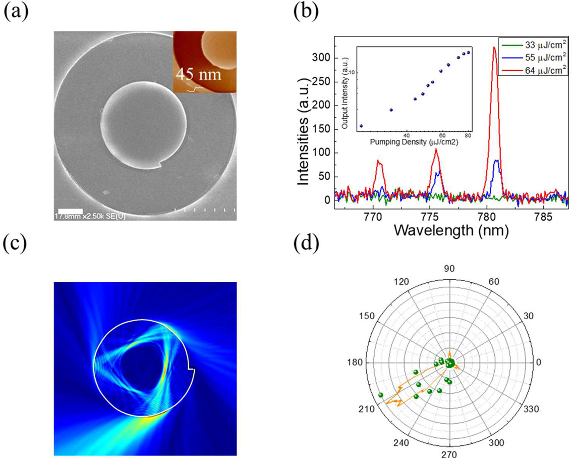
Consequently, whispering gallery mode (WGM) micro-lasers with
well-controlled mode numbers, mode spacing, repeatability, directionalities,
and even internal angular momentum are experimentally realized. In addition,
by constructing coupled micro-structures, the proximity effffects between
WGM lasers are also explored. This research provides a substrate-control
mechanism to precisely defifine and control MAPbX
3
perovskite micro-lasers.